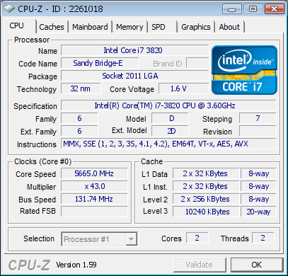
GUN'G'STAR of TeamRussia successfully achieved an overclocking record of
5.666 GHz for the quad-core Intel Core i7-3820 processor; a feat that
validates the LGA2011 i7-3820 of being a generally good chip for
overclocking, despite being "Limited Unlocked" (BClk multiplier being
unlocked only to a few notches above its stock setting). GUN'G'STAR
achieved a clock speed of 5,665.99 MHz using a BClk speed of 131.74 MHz,
a multiplier value of 43x, and core voltage of 1.6V. The chip was
assisted with GeIL-made DDR3-1600 memory sitting on all four channels,
and ASUS Rampage IV Extreme motherboard. Only 2 out of 4 cores of the
i7-3820 were enabled for the feat, HyperThreading was disabled. Extreme
cooling was used. The CPU-Z validation can be accessed here.
Source: Expreview
Showing posts with label Intel. Show all posts
Friday, February 24, 2012
Friday, February 17, 2012
Mass Shipments of Ivy Bridge Delayed to June
In what could come as a disappointment to some, Intel has reportedly put
off mass-shipments of its third-generation Core processors (codenamed
"Ivy Bridge") to June. The company, however, will go ahead with its
April launch schedule, and will issue small shipments of these chips.
This information comes from sources among notebook manufacturers.
This delay, however, doesn't appear to be linked to Intel's ability to ship the new 22 nm chips. Sources say that most notebooks vendors are having a very hard time digesting inventories of current-generation "Sandy Bridge" Core processors, and so the delay is merely to help them ship the last of their notebooks running current-generation chips, and to minimize the impact of the onset of new chips. Notebook vendors are currently seeing lukewarm demand.
Source: DigiTimes, Image Courtesy: LegitReviews
This delay, however, doesn't appear to be linked to Intel's ability to ship the new 22 nm chips. Sources say that most notebooks vendors are having a very hard time digesting inventories of current-generation "Sandy Bridge" Core processors, and so the delay is merely to help them ship the last of their notebooks running current-generation chips, and to minimize the impact of the onset of new chips. Notebook vendors are currently seeing lukewarm demand.
Source: DigiTimes, Image Courtesy: LegitReviews
Wednesday, February 15, 2012
Ivy Bridge Desktop Core i3 Processor Lineup Detailed, Lack PCIe Gen. 3.0
Details of desktop Core i7 and Core i5 "Ivy Bridge" processors in the LGA1155 package have been detailed
at lengths, in the past. Core i3 parts based on the same 22 nm Ivy
Bridge silicon, however, were relatively known. Tables listing out
updated information about the lineup points out that Intel has as many
as five Core i3 "Ivy Bridge" desktop processors in the works, all
dual-core, and among which two are low-power parts.
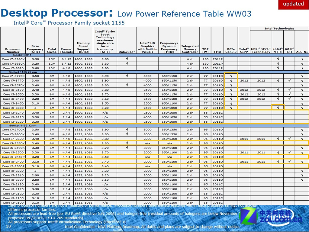
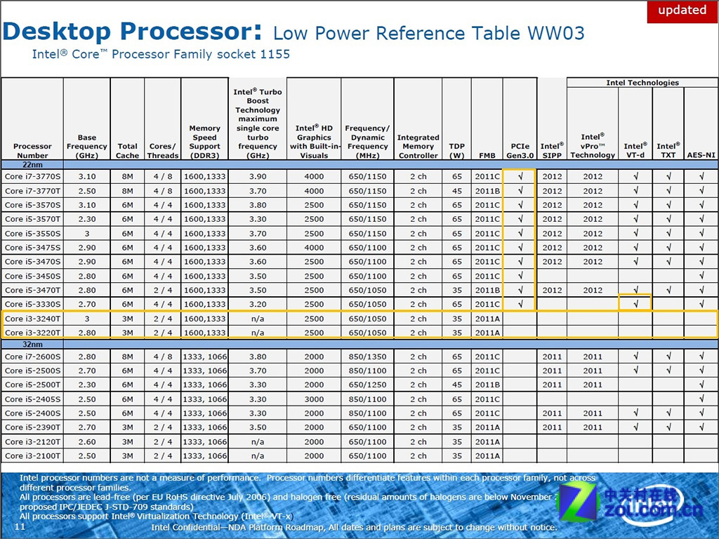
The table also suggests that these Core i3 chips will have reduced features, importantly, the lack of PCI-Express 3.0 bus. When connected to these chips, PCI-E 3.0 add-on cards (such as graphics cards) will function in PCI-Express 2.0 mode. Further, these chips will lack support for AES-NI (accelerates encryption), VT-d (enhanced virtualization), and TXT (security). Certain models in the lineup have faster integrated graphics, denoted by a "5" in the end of the model number. These chips also lack Turbo Boost for the x86 cores, but feature HyperThreading.
Leading the pack is Core i3-3240, clocked at 3.40 GHz, with integrated graphics clocked at 650 MHz / 1020 MHz Dynamic. This is followed by the Core i3-3225, which is clocked at 3.30 GHz, packing faster Intel HD 4000 graphics. The Core i3-3220 is likely the cheapest of the lot, also clocked at 3.30 GHz, but with slower HD 2500 graphics. These three chips have rated TDP of 55W. Moving on to the low-power models, which have 35W TDP, we have the Core i3-3240T, with 3.00 GHz clock speed, and Core i3-3220T, with 2.80 GHz clock speed.
Sources: Zol.com.cn, VR-Zone
The table also suggests that these Core i3 chips will have reduced features, importantly, the lack of PCI-Express 3.0 bus. When connected to these chips, PCI-E 3.0 add-on cards (such as graphics cards) will function in PCI-Express 2.0 mode. Further, these chips will lack support for AES-NI (accelerates encryption), VT-d (enhanced virtualization), and TXT (security). Certain models in the lineup have faster integrated graphics, denoted by a "5" in the end of the model number. These chips also lack Turbo Boost for the x86 cores, but feature HyperThreading.
Leading the pack is Core i3-3240, clocked at 3.40 GHz, with integrated graphics clocked at 650 MHz / 1020 MHz Dynamic. This is followed by the Core i3-3225, which is clocked at 3.30 GHz, packing faster Intel HD 4000 graphics. The Core i3-3220 is likely the cheapest of the lot, also clocked at 3.30 GHz, but with slower HD 2500 graphics. These three chips have rated TDP of 55W. Moving on to the low-power models, which have 35W TDP, we have the Core i3-3240T, with 3.00 GHz clock speed, and Core i3-3220T, with 2.80 GHz clock speed.
Sources: Zol.com.cn, VR-Zone
Intel’s Next-Generation Communications Platform Key to Accelerated Network Services
Intel Corporation today disclosed several significant features for the
company's next-generation communications platform, codenamed "Crystal
Forest." Building upon Intel's strong presence in communications
infrastructure, the platform will handle data processing across the
network more efficiently and securely, while addressing the specialized
needs for handling cloud connectivity and content processing.
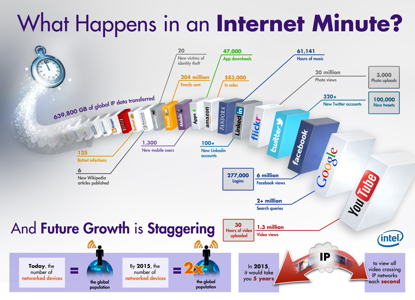
Each minute of the day, 30 hours of video are uploaded across the network, and by 2015 it is estimated to take 5 years to watch all the video crossing IP networks each second. As these numbers continue to climb, the burden will be on equipment manufacturers and service providers to deliver platform solutions that can cost-effectively manage rapidly increasing traffic without compromising performance and security.
Currently, equipment manufacturers must combine a variety of highly specialized silicon co-processors with different software programming models to handle multiple communications workloads when building platforms for a scalable network - a very complex and expensive endeavor. With Crystal Forest, equipment manufacturers will be able to consolidate three communications workloads - application, control and packet processing - on multi-core Intel architecture processors to deliver better performance and accelerate time to market. They can also develop a scalable product line based on multiple Intel processor options to plan for future performance increases.
"The demand for increased network performance will continue to grow as more smart devices connect to the Internet every day," said Rose Schooler, general manager of Intel's Communications Infrastructure Division. "And with the popularity of social networking and other high-bandwidth services, such as video and photo uploads/downloads, interactive video, crowdcasting and online gaming, service providers will be challenged to efficiently provision sufficient upstream capacity and manage the spike in network traffic."
Intel's next-generation communications platform, Crystal Forest, is expected to deliver up to 160 million packets per second performance for Layer 3 packet forwarding, making it possible to send thousands of high-definition videos across each network node. Previously, only ASIC or specialized processors were capable of sending more than 100 million packets per second. The Intel Data Plane Development Kit, a set of software libraries and algorithms, improves the performance and throughput of packets on Intel architecture platforms to yield more than five times the performance over previous generations of Intel platforms.
Crystal Forest will also utilize Intel QuickAssist technology, which processes and accelerates specialized packet workloads - cryptography, compression and deep packet inspection included – on standard Intel platforms. Using this technology, secure Internet transactions can be accelerated up to 100 Gbps on the platform to give service providers the ability to handle many more secure transactions and without the cost of specialized solutions. The network will also be able to evolve to provide "always-on" secure Internet connections, as opposed to the opt-in connections currently used on select applications or for financial transactions online.
Designed to Grow with the Network
The Crystal Forest platform will enable equipment manufacturers to design more flexible platforms, from small- to medium-sized business firewalls to high-end routers. Service providers, too, can save money by deploying fewer complex platforms, making their network easier to manage and maintain. The Intel platform roadmap plans to deliver annual performance refreshes for several years, so equipment manufacturers and service providers will be able to scale and refresh their designs to meet future network needs. Additionally, Crystal Forest will use a common application programming interface and common drivers so that multiple designs can be implemented in much less time and at much lower development costs.
Full System Simulation of the Crystal Forest Platform
Developers can accelerate software development, testing and integration by utilizing a simulation model of the Crystal Forest platform provided by Wind River Simics. With Simics, users can model any Crystal Forest target configuration and then run unmodified target software on that model. Wind River Simics enables developers to do BIOS bring-up, operating-system optimization and application development more efficiently.
The new platform is scheduled to be available later in 2012.
Source
Each minute of the day, 30 hours of video are uploaded across the network, and by 2015 it is estimated to take 5 years to watch all the video crossing IP networks each second. As these numbers continue to climb, the burden will be on equipment manufacturers and service providers to deliver platform solutions that can cost-effectively manage rapidly increasing traffic without compromising performance and security.
Currently, equipment manufacturers must combine a variety of highly specialized silicon co-processors with different software programming models to handle multiple communications workloads when building platforms for a scalable network - a very complex and expensive endeavor. With Crystal Forest, equipment manufacturers will be able to consolidate three communications workloads - application, control and packet processing - on multi-core Intel architecture processors to deliver better performance and accelerate time to market. They can also develop a scalable product line based on multiple Intel processor options to plan for future performance increases.
"The demand for increased network performance will continue to grow as more smart devices connect to the Internet every day," said Rose Schooler, general manager of Intel's Communications Infrastructure Division. "And with the popularity of social networking and other high-bandwidth services, such as video and photo uploads/downloads, interactive video, crowdcasting and online gaming, service providers will be challenged to efficiently provision sufficient upstream capacity and manage the spike in network traffic."
Intel's next-generation communications platform, Crystal Forest, is expected to deliver up to 160 million packets per second performance for Layer 3 packet forwarding, making it possible to send thousands of high-definition videos across each network node. Previously, only ASIC or specialized processors were capable of sending more than 100 million packets per second. The Intel Data Plane Development Kit, a set of software libraries and algorithms, improves the performance and throughput of packets on Intel architecture platforms to yield more than five times the performance over previous generations of Intel platforms.
Crystal Forest will also utilize Intel QuickAssist technology, which processes and accelerates specialized packet workloads - cryptography, compression and deep packet inspection included – on standard Intel platforms. Using this technology, secure Internet transactions can be accelerated up to 100 Gbps on the platform to give service providers the ability to handle many more secure transactions and without the cost of specialized solutions. The network will also be able to evolve to provide "always-on" secure Internet connections, as opposed to the opt-in connections currently used on select applications or for financial transactions online.
Designed to Grow with the Network
The Crystal Forest platform will enable equipment manufacturers to design more flexible platforms, from small- to medium-sized business firewalls to high-end routers. Service providers, too, can save money by deploying fewer complex platforms, making their network easier to manage and maintain. The Intel platform roadmap plans to deliver annual performance refreshes for several years, so equipment manufacturers and service providers will be able to scale and refresh their designs to meet future network needs. Additionally, Crystal Forest will use a common application programming interface and common drivers so that multiple designs can be implemented in much less time and at much lower development costs.
Full System Simulation of the Crystal Forest Platform
Developers can accelerate software development, testing and integration by utilizing a simulation model of the Crystal Forest platform provided by Wind River Simics. With Simics, users can model any Crystal Forest target configuration and then run unmodified target software on that model. Wind River Simics enables developers to do BIOS bring-up, operating-system optimization and application development more efficiently.
The new platform is scheduled to be available later in 2012.
Source
Tuesday, February 14, 2012
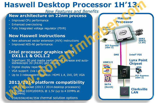
Intel Haswell Packs DirectX 11.1 Graphics
Intel will launch its new processor architecture, codenamed "Haswell",
which will go on to succeed "Ivy Bridge". More than an year away from
its market entry, Haswell has already been exhaustively
documented, but not many got into the details about its embedded
graphics processor. That is, until now. A new internal slide sourced by
DonanimHaber details the integrated GPU (iGPU), it appears like Intel
has solid plans for home users.
To begin with, Haswell's iGPU will be DirectX 11.1 compliant, which means it will take advantage of API optimizations that improve performance, for typical desktop usage scenarios. Apart from support for a new DirectCompute architecture, it will also support OpenCL 1.2, which speeds up certain GPGPU-optimized applications. More importantly, the iGPU will be designed around a new stereoscopic 3D standard called Auto-Stereoscopic 3D (AS3D), which will take the likes of Blu-ray 3D acceleration, stereo 3D photos, etc., to the masses. Currently, it takes at least an entry-level GeForce or Radeon GPU to for acceptable performance with stereo 3D.
Another significant change is what Intel refers to as "digital display repartition". Until now, Intel processors with embedded graphics relied on the PCH to perform all display I/O functions, the iGPU communicates to the PCH over the Flexible Display Interface (FDI), a special data link dedicated to this function. With Haswell, digital display outputs (such as DVI, HDMI, DisplayPort), will be wired directly to the CPU socket, while analog display (such as D-Sub), will be handled by a RAMDAC located in the PCH, to which a digital signal is sent over FDI. This design ensures there's no performance bottleneck with higher resolution digital displays, while at the same time, ensuring analog display quality isn't affected by the RAMDAC being located in the GPU die, where it's bound for interference by some pretty high-current circuits.
Source: DonanimHaber
To begin with, Haswell's iGPU will be DirectX 11.1 compliant, which means it will take advantage of API optimizations that improve performance, for typical desktop usage scenarios. Apart from support for a new DirectCompute architecture, it will also support OpenCL 1.2, which speeds up certain GPGPU-optimized applications. More importantly, the iGPU will be designed around a new stereoscopic 3D standard called Auto-Stereoscopic 3D (AS3D), which will take the likes of Blu-ray 3D acceleration, stereo 3D photos, etc., to the masses. Currently, it takes at least an entry-level GeForce or Radeon GPU to for acceptable performance with stereo 3D.
Another significant change is what Intel refers to as "digital display repartition". Until now, Intel processors with embedded graphics relied on the PCH to perform all display I/O functions, the iGPU communicates to the PCH over the Flexible Display Interface (FDI), a special data link dedicated to this function. With Haswell, digital display outputs (such as DVI, HDMI, DisplayPort), will be wired directly to the CPU socket, while analog display (such as D-Sub), will be handled by a RAMDAC located in the PCH, to which a digital signal is sent over FDI. This design ensures there's no performance bottleneck with higher resolution digital displays, while at the same time, ensuring analog display quality isn't affected by the RAMDAC being located in the GPU die, where it's bound for interference by some pretty high-current circuits.
Source: DonanimHaber
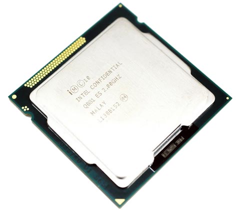
Core i7-3820 Sandy Bridge-E Starts Selling in Japan
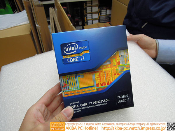
Intel's most affordable processor in the LGA2011 package, the Core
i7-3820, surfaced on Japanese stores in the Akihabara electronics
shopping district of Tokyo. It is priced around 25,000 JPY (US $322).
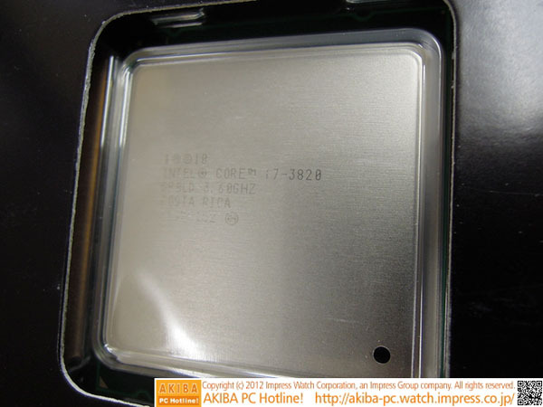
The retail box of this chip, carrying the S-Spec code "SR0LD", appears
to be as big as those of the Core i7-3930K and Core i7-3960X Extreme
Edition, its shape indicates that it lacks a bundled cooling solution,
and so users should still rely on compatible third-party coolers, or use
Intel's RTS2011LC, purchased separately.
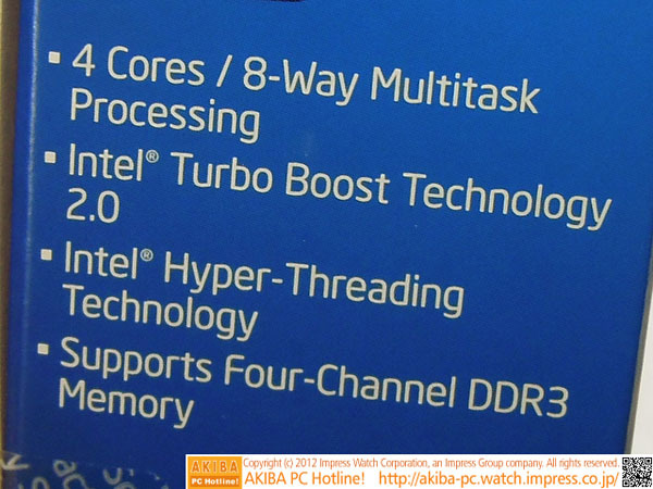
The Core i7-3820 is a quad-core part carved out of the Sandy Bridge-E silicon. It has four cores, and eight logical CPUs enabled with HyperThreading Technology. The chip is clocked at 3.60 GHz. Caches include 256 KB L2 per core, and 10 MB shared L3. The chip retains the quad-channel DDR3 IMC present on the more expensive six-core parts. It is also said to be "limited unlocked", meaning it allows multiplier-assisted overclocking to a certain limit. The Core i7-3820 is not officially launched, though it should be unofficially supported by most socket LGA2011 motherboards based on the X79 chipset.
Source: PCWatch Akiba
The Core i7-3820 is a quad-core part carved out of the Sandy Bridge-E silicon. It has four cores, and eight logical CPUs enabled with HyperThreading Technology. The chip is clocked at 3.60 GHz. Caches include 256 KB L2 per core, and 10 MB shared L3. The chip retains the quad-channel DDR3 IMC present on the more expensive six-core parts. It is also said to be "limited unlocked", meaning it allows multiplier-assisted overclocking to a certain limit. The Core i7-3820 is not officially launched, though it should be unofficially supported by most socket LGA2011 motherboards based on the X79 chipset.
Source: PCWatch Akiba
Friday, February 10, 2012
Intel Haswell In Bound for March-April 2013
As Intel's tick-tock CPU development Juggernaut rolls on, things seem
very much on track, looking into the near future. Intel will launch its
new "Ivy Bridge" 3rd Generation Core processor family in early-April
2012, which is a miniaturization of what is essentially the "Sandy
Bridge" to the new 22 nm process, with IPC and instruction-set
improvements, along with a faster graphics controller. The new process
will also up clock speeds and overclocking headroom for chips that
support it. What's more interesting, though, is that the architecture
that succeeds Ivy Bridge, codenamed "Haswell", will be less than an year
away in April...well almost.
A roadmap slide sourced by DonanimHaber pins the launch of Haswell to March-April, 2013. Haswell is a brand new CPU architecture that will succeed Ivy Bridge. According to the conventional idea of Intel's tick-tock CPU development strategy, it will be built on the 22 nm fab process, which will have gained some maturity by then. Intel follows a "tick-tock" product development model. Every year, Intel's product lineup sees either of the two. A "tock" brings in a new x86 architecture, a "tick" miniaturizes it to a newer silicon fabrication process. Earlier reports indicated that Haswell Core processors will be based on a newer socket, the LGA1150, and hence it will not be compatible with LGA1155 platforms.
Source: DonanimHaber
A roadmap slide sourced by DonanimHaber pins the launch of Haswell to March-April, 2013. Haswell is a brand new CPU architecture that will succeed Ivy Bridge. According to the conventional idea of Intel's tick-tock CPU development strategy, it will be built on the 22 nm fab process, which will have gained some maturity by then. Intel follows a "tick-tock" product development model. Every year, Intel's product lineup sees either of the two. A "tock" brings in a new x86 architecture, a "tick" miniaturizes it to a newer silicon fabrication process. Earlier reports indicated that Haswell Core processors will be based on a newer socket, the LGA1150, and hence it will not be compatible with LGA1155 platforms.
Source: DonanimHaber
Tuesday, February 7, 2012
Intel Debuts the 520 Series SATA 6.0 Gbps Solid State Drives
Intel Corporation announced today its fastest, most robust
client/consumer solid-state drive (SSD) to date, the Intel Solid-State
Drive 520 Series (Intel SSD 520), a 6 gigabit-per-second (gbps) SATA III
SSD produced using Intel compute-quality 25-nanometer (nm) NAND memory
process technology. Aimed at delivering world-class performance for even
the most demanding PC enthusiasts, gamers, professionals or
small-medium businesses (SMBs), the Intel SSD 520 has fast throughput
performance, new security features and unmatched reliability to meet
even the most intensive user requirements.
Any consumer application requiring high throughput and bandwidth, low latencies and accelerated speed will benefit from the Intel SSD 520. Software developers, architects, accountants, engineers, musicians, media creators and artists are just some of the professionals that will find that the Intel SSD 520's full package of features can make a dramatic impact on their productivity. With faster performance for graphic renderings, compiling, data transfers and system boot-ups, users can speed through multi-tasking or once-cumbersome application wait times with an Intel SSD 520 Series.
"We tapped Intel engineering to create a client SSD that delivers performance on all fronts with obsessively high reliability," said Rob Crooke, Intel vice president and general manager of the Intel Non-Volatile Memory Solutions Group. "The Intel SSD 520 once again raises the industry bar on SSD performance, quality and reliability to dramatically improve user experience."
Unlike a traditional hard disk drive (HDD) with spinning disks and moveable parts, an SSD is based on silicon, NAND flash memory specifically, to create a lower power, more reliable and drastically faster storage solution that can keep up with today's most demanding applications, Internet streaming and intense multi-tasking. Based on its own industry-leading 25 nm Intel compute-quality NAND flash memory and a 6 gbps SATA III interface, the Intel SSD 520 uses an LSI SandForce Flash Storage Processor with an Intel co-defined and validated firmware release, to create an SSD that sets new industry performance benchmarks. The Intel SSD 520 delivers up to 80,000 maximum 4K random write Input-Output Operations Per Second (IOPS) and up to 50,000 4K random read IOPS to speed through every day operations. High sequential read performance of up to 550 megabytes-per-second (MB/s) and up to 520 MB/s sequential writes also markedly accelerate and improve user productivity. This is backed by thousands of hours of Intel testing and validation, including more than 5,000 individual tests, as well as a 5-year limited warranty.
"We worked closely with Intel to leverage their deep understanding of the NAND flash, ultimately providing a unique and optimized solution for client computing applications with the LSI SandForce Flash Storage Processor," said Michael Raam, vice president and general manager of LSI's Flash Components Division, formed by LSI's acquisition of SandForce. "Working through Intel's extensive validation process ensures the Intel 520 SSD will raise the bar in delivering top-tier performance and superior quality and reliability over the life of the drive."
The Intel SSD 520 will mark the high end of its client SSD offerings and include these new features: a wide range of user capacities from 60 GB to 480 GB, Advanced Encryption Standard (AES) 256 bit encryption capabilities and stronger password protection for added security in the event of theft or power loss. According to PCMark Vantage benchmarking, users of the Intel SSD 520 may see significant productivity gains through an up to 78 percent boost in overall PC responsiveness, and gamers will see an up to 88 percent jump in performance to enhance their gaming experience. IT professionals will not only provide this additional performance and productivity to their customers/employees, but find that the Intel SSD 520 also delivers on reliability, improved security, smoother operations and lower total operational costs.
"Our game development workflow involves a combination of large batch process and aggressive interactive pre-visualization, all highly parallelized to the point that the storage performance becomes a major bottleneck," said John Carmack, founder and technical director of id* Software, a gaming software developer and creators of Doom and Quake. "For many of our workloads, Intel SSDs have doubled throughput, and in some cases involving mapping tens of gigabytes of image data, we have seen an honest order of magnitude performance improvement, which is a rare and wonderful thing."
With a broad range of capacity choices, the Intel SSD 520 Series is priced as follows, based on 1,000-unit quantities: 60 GB for $149, 120 GB at $229, 180 GB at $369, 240 GB at $509 and 480 GB at $999. It comes with a 5-year limited warranty.
Source
Any consumer application requiring high throughput and bandwidth, low latencies and accelerated speed will benefit from the Intel SSD 520. Software developers, architects, accountants, engineers, musicians, media creators and artists are just some of the professionals that will find that the Intel SSD 520's full package of features can make a dramatic impact on their productivity. With faster performance for graphic renderings, compiling, data transfers and system boot-ups, users can speed through multi-tasking or once-cumbersome application wait times with an Intel SSD 520 Series.
"We tapped Intel engineering to create a client SSD that delivers performance on all fronts with obsessively high reliability," said Rob Crooke, Intel vice president and general manager of the Intel Non-Volatile Memory Solutions Group. "The Intel SSD 520 once again raises the industry bar on SSD performance, quality and reliability to dramatically improve user experience."
Unlike a traditional hard disk drive (HDD) with spinning disks and moveable parts, an SSD is based on silicon, NAND flash memory specifically, to create a lower power, more reliable and drastically faster storage solution that can keep up with today's most demanding applications, Internet streaming and intense multi-tasking. Based on its own industry-leading 25 nm Intel compute-quality NAND flash memory and a 6 gbps SATA III interface, the Intel SSD 520 uses an LSI SandForce Flash Storage Processor with an Intel co-defined and validated firmware release, to create an SSD that sets new industry performance benchmarks. The Intel SSD 520 delivers up to 80,000 maximum 4K random write Input-Output Operations Per Second (IOPS) and up to 50,000 4K random read IOPS to speed through every day operations. High sequential read performance of up to 550 megabytes-per-second (MB/s) and up to 520 MB/s sequential writes also markedly accelerate and improve user productivity. This is backed by thousands of hours of Intel testing and validation, including more than 5,000 individual tests, as well as a 5-year limited warranty.
"We worked closely with Intel to leverage their deep understanding of the NAND flash, ultimately providing a unique and optimized solution for client computing applications with the LSI SandForce Flash Storage Processor," said Michael Raam, vice president and general manager of LSI's Flash Components Division, formed by LSI's acquisition of SandForce. "Working through Intel's extensive validation process ensures the Intel 520 SSD will raise the bar in delivering top-tier performance and superior quality and reliability over the life of the drive."
The Intel SSD 520 will mark the high end of its client SSD offerings and include these new features: a wide range of user capacities from 60 GB to 480 GB, Advanced Encryption Standard (AES) 256 bit encryption capabilities and stronger password protection for added security in the event of theft or power loss. According to PCMark Vantage benchmarking, users of the Intel SSD 520 may see significant productivity gains through an up to 78 percent boost in overall PC responsiveness, and gamers will see an up to 88 percent jump in performance to enhance their gaming experience. IT professionals will not only provide this additional performance and productivity to their customers/employees, but find that the Intel SSD 520 also delivers on reliability, improved security, smoother operations and lower total operational costs.
"Our game development workflow involves a combination of large batch process and aggressive interactive pre-visualization, all highly parallelized to the point that the storage performance becomes a major bottleneck," said John Carmack, founder and technical director of id* Software, a gaming software developer and creators of Doom and Quake. "For many of our workloads, Intel SSDs have doubled throughput, and in some cases involving mapping tens of gigabytes of image data, we have seen an honest order of magnitude performance improvement, which is a rare and wonderful thing."
With a broad range of capacity choices, the Intel SSD 520 Series is priced as follows, based on 1,000-unit quantities: 60 GB for $149, 120 GB at $229, 180 GB at $369, 240 GB at $509 and 480 GB at $999. It comes with a 5-year limited warranty.
Source
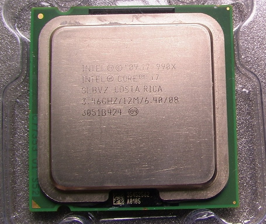
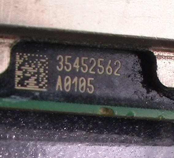
Fake Core i7-990X Surfaces on Forums
A scamster has managed to pull off a fake "Intel Core i7-990X"
processor. An unsuspecting buyer paid hundreds of dollars for a Core
i7-990X six-core LGA1366 processor, only to end up with a badly-done
fake. The fake chip is a worthless LGA775 Pentium, on which the IHS
markings of a Core i7-990X have been etched. Intel and AMD put tiny
windows on their retail processor boxes so buyers could see these
markings before breaking open the company seal. At least in the case of
Intel's product boxes, the windows aren't big enough to let you see the
entire CPU package. In case of this chip, the buyer couldn't have
spotted that the chip was an LGA775 (and not LGA1366), and couldn't spot
the 3D hologram and serial number sticker that's found on the obverse
side of the package, under the IHS. The thread where this fake was
reported can be read here.
Source: CPU World
Source: CPU World
Friday, February 3, 2012
10-core Ivy Bridge-EP Sample Tested
The Ivy Bridge LGA1155 processors inbound for April are mom and pop PC
chips in front of the monstrosities Intel has planned for the enterprise
(and possibly high-end desktop/HEDT) markets, based on the
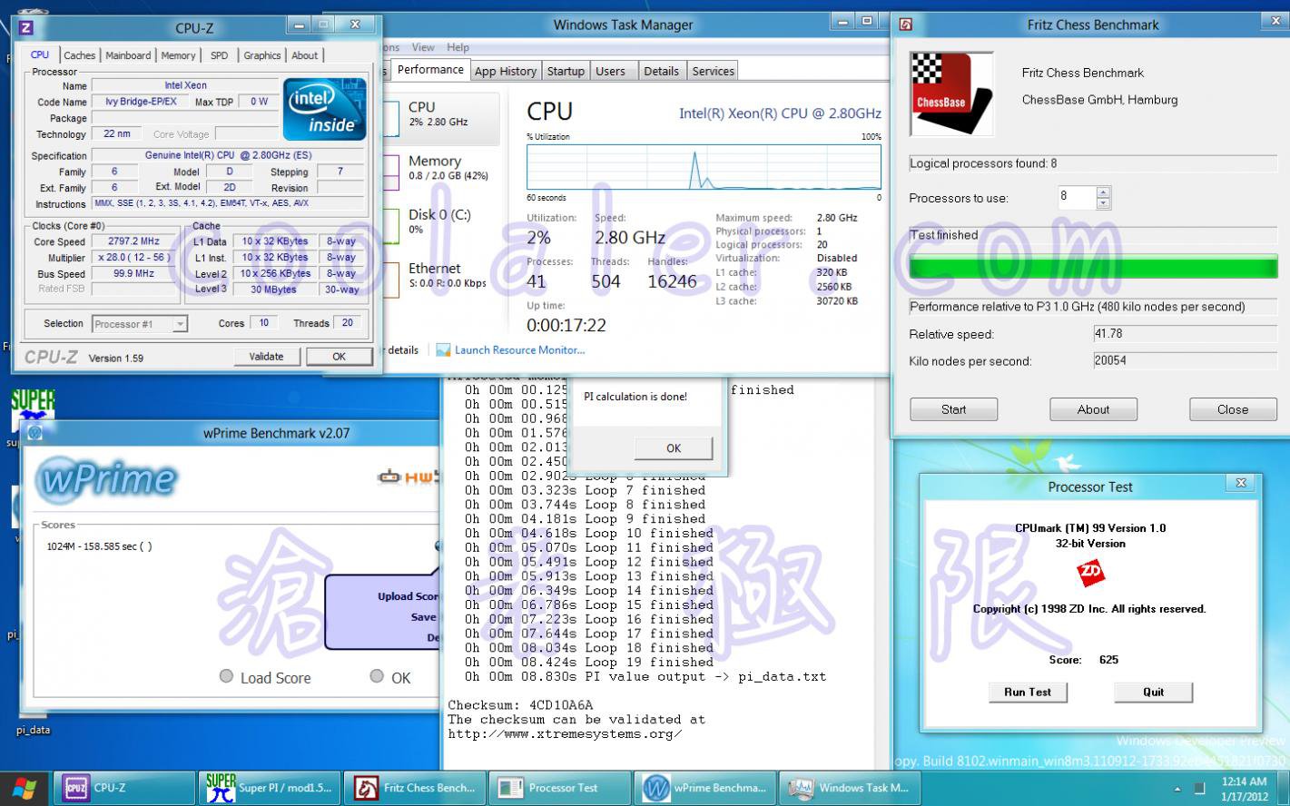
architecture. An 10-core Ivy Bridge-EP engineering sample, made it to
the right hands in Taiwan (wrong hands for Intel), that wasted no time
in putting them through some tests.
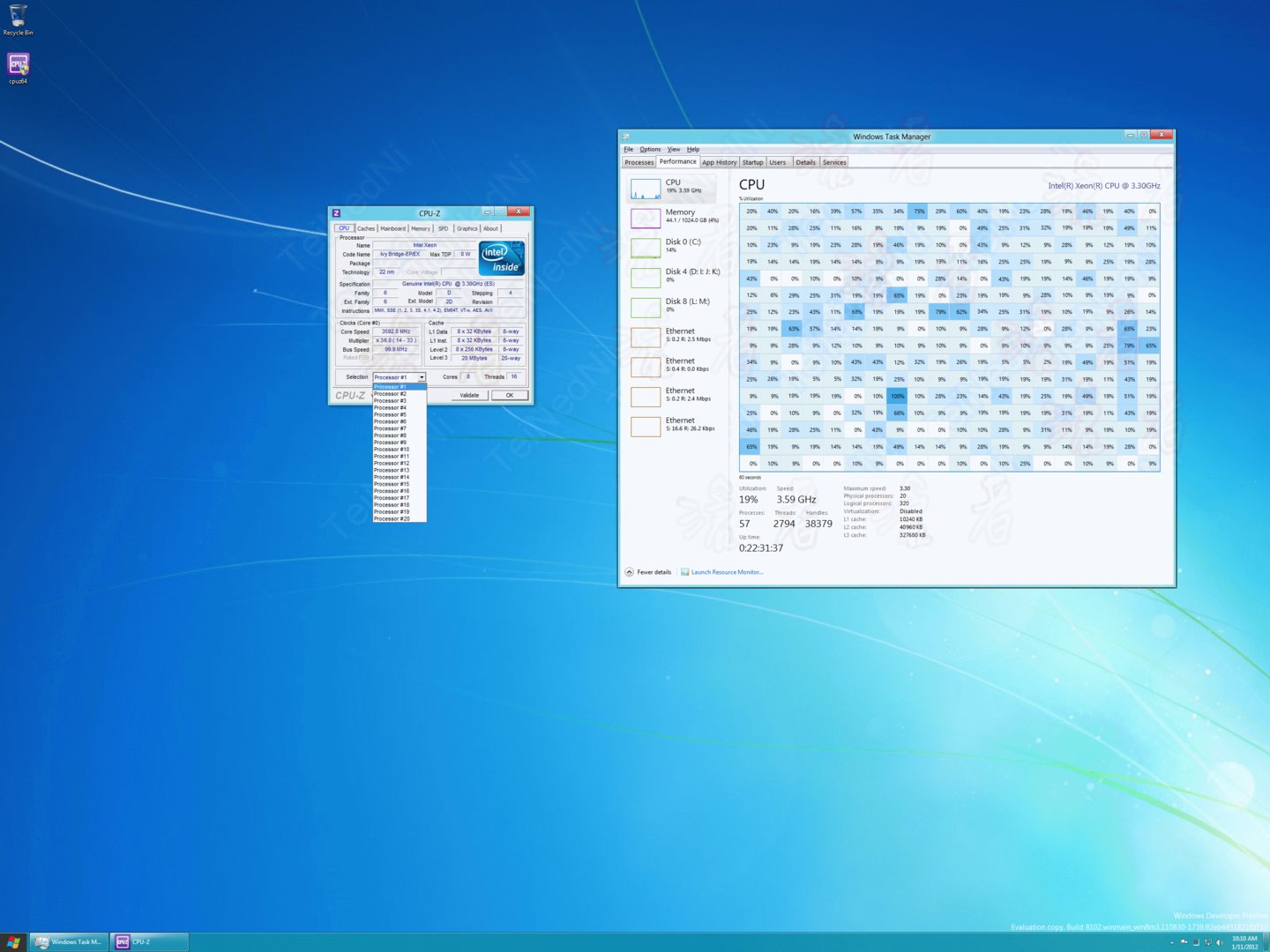
The 10-core Ivy Bridge-EP/EX chip features 10 next-generation cores clocked at 2.80 GHz, with 256 KB L2 cache per core, 30 MB shared L3 cache, and HyperThreading technology that enables 20 logical CPUs. This chip crunched WPrime 1024M in 158.5 seconds, and scores 41.78X relative speed in Fritz chess when just 8 of its 20 threads are put to use. You can also find some pretty screen shots of CPU-Z with its long processor selection list and Windows 8 task manager.
Sources: Coolaler, ComputerBase.de
The 10-core Ivy Bridge-EP/EX chip features 10 next-generation cores clocked at 2.80 GHz, with 256 KB L2 cache per core, 30 MB shared L3 cache, and HyperThreading technology that enables 20 logical CPUs. This chip crunched WPrime 1024M in 158.5 seconds, and scores 41.78X relative speed in Fritz chess when just 8 of its 20 threads are put to use. You can also find some pretty screen shots of CPU-Z with its long processor selection list and Windows 8 task manager.
Sources: Coolaler, ComputerBase.de
Tuesday, January 31, 2012
Intel Releases Seven More 32 nm Processors
US chip giant Intel has now added seven new processors to its portfolio,
the Core i5-2550K, i5-2450P and i5-2380P targeting desktops, and the
Celeron B815, B720, 867 and 797 for mobile PCs.
The Core i5-2550K costs $225 ($9 more than the i5-2500K) and features four cores @ 3.4 GHz (the 2500K has a base clock of 3.3 GHz), four threads, 6 MB of L3 cache and a TDP of 95W. The i5-2450P ($195) and i5-2380P ($177) have similar specs, expect their base clock is 3.2 GHz and 3.1 GHz, respectively.
The Celeron B815 has two cores @ 1.6 GHz, two threads, 2 MB of L3 cache and bears a price tag of $86, while the B720, which costs $70, has one core clocked at 1.7 GHz, one thread and 1 MB of L3 cache.
The ULV (ultra-low voltage) Celeron 867 and 797 cost $134 and $107, respectively. The former packs two cores @ 1.3 GHz, two threads, 2 MB L3 cache, whereas the latter has just one core @ 1.4 GHz, one thread, and 1 MB of L3 cache.
Source
The Core i5-2550K costs $225 ($9 more than the i5-2500K) and features four cores @ 3.4 GHz (the 2500K has a base clock of 3.3 GHz), four threads, 6 MB of L3 cache and a TDP of 95W. The i5-2450P ($195) and i5-2380P ($177) have similar specs, expect their base clock is 3.2 GHz and 3.1 GHz, respectively.
The Celeron B815 has two cores @ 1.6 GHz, two threads, 2 MB of L3 cache and bears a price tag of $86, while the B720, which costs $70, has one core clocked at 1.7 GHz, one thread and 1 MB of L3 cache.
The ULV (ultra-low voltage) Celeron 867 and 797 cost $134 and $107, respectively. The former packs two cores @ 1.3 GHz, two threads, 2 MB L3 cache, whereas the latter has just one core @ 1.4 GHz, one thread, and 1 MB of L3 cache.
Source
Tuesday, January 3, 2012
Dishonest Intel OEM Engineers To Get Five Years Behind Bars
The Taiwan Criminal Investigation Bureau has been doing a bit of
investigating and has arrested four engineers working for Intel's OEM
partners (names not disclosed) for flogging Engineering Sample (ES)
processors on eBay. ES processors are intended strictly for
qualification testing purposes for development of new products by OEM's
and are only loaned to them under strict non-disclosure agreements,
hence putting these on eBay is illegal. The Bureau searched the suspects
houses last month and found 178 ES CPU's, worth around $800,000. Note
that this value seems to be somewhat high, as it would make each CPU
worth around $4,500. We will update this article if new values come to
light. Also, this is not a new operation that has been busted, since the
suspects had admitted to selling around 500 ES CPU's since 2009. For
their efforts, the fab four now face five years in prison.
It should be noted for anyone contemplating the purchase of such dodgy CPU's on eBay or similar places, that they may be overstressed and contain faults, due to the intensive and sometimes destructive testing they go through. Just don't do it, kids.
Source: TechEYE
It should be noted for anyone contemplating the purchase of such dodgy CPU's on eBay or similar places, that they may be overstressed and contain faults, due to the intensive and sometimes destructive testing they go through. Just don't do it, kids.
Source: TechEYE
Intel to Roll Out 40 New Server Processors in H1 2012
With key enterprise architectures such as Sandy Bridge-EP awaiting
launch, Intel has as many as 40 Xeon processor models to release in the
first half of 2012, which it will likely launch in two rounds of 20
models, for each of the first two quarters of this year. In Q1, Intel
will release six-core Xeon E5-1660 and E5-1650, and a yet to be named
quad-core model; the three will be priced at US US$1,080, US$583 and
US$294, respectively. In the same quarter, Intel will also launch 7
eight-core Xeon processor models, including the Xeon E5-2690four
six-core processors including E5-2640, three quad-core processors
including E5-2609 and dual-core processor E5-2637. Intel will also
launch some low-power (energy-efficient) Xeon models, including Xeon
E5-2450L and six-core E5-2430L priced at US$1,106 and US$662.
In the second quarter of 2012, Intel will launch the other 20 models. These include Xeon processors based on the Ivy Bridge silicon, and in the socket H2 (LGA1155) package. The Xeon E3-1290v2 is an example of such a chip. These high-grade Ivy Bridge chips will be priced in the range of US$189-884. Then on, 7 more E5 series models will be launched, including Xeon E5-2470, priced between US$192-1,440. Towards the end of the quarter, Intel will launch low-power eight-core and six-core Xeon processor models, including Xeon E5-2650L and E5-2630L, priced at priced at US$1,106 and US$662, respectively.
Source: DigiTimes
In the second quarter of 2012, Intel will launch the other 20 models. These include Xeon processors based on the Ivy Bridge silicon, and in the socket H2 (LGA1155) package. The Xeon E3-1290v2 is an example of such a chip. These high-grade Ivy Bridge chips will be priced in the range of US$189-884. Then on, 7 more E5 series models will be launched, including Xeon E5-2470, priced between US$192-1,440. Towards the end of the quarter, Intel will launch low-power eight-core and six-core Xeon processor models, including Xeon E5-2650L and E5-2630L, priced at priced at US$1,106 and US$662, respectively.
Source: DigiTimes
Friday, December 30, 2011
Intel Plans to Launch Medfield Platform in Q2, Clover Trail-W platform in Q4, 2012
According to the latest information received by industry observer
DigiTimes, Intel plans to launch the first processor platform for
ultra-thin Android tablets based on its x86 architecture, codenamed
"Medfield", in Q2 2012. Tablets based on this will be able to run
Android 4.0 "Ice Cream Sandwich". Then in Q4 2012, Intel plans to launch
the more powerful Clover Trail-W platform. Currently, Intel's Oak Trail
platform consisting of Atom Z670 processor and SM35 chipset drive
Windows 7 or Android Honeycomb tablets.
The fundamental difference between Medfield and Clover Trail-W with its predecessor Oak Tail, is that Medfield will be designed for ultra-thin tablets with long batter life, currently only ARM processors provide the kind of performance-per-Watt to achieve this form-factor. Oak Trail and its succeeding Clover Trail-W, are designed for slightly more capable tablets. Oak Trail is opted today, to design tablets that run Windows 7 PC operating system. Microsoft will design performance and UI-optimized Windows 8 variants when its next-gen operating system sees the light of the day next year.
Source: DigiTimes
The fundamental difference between Medfield and Clover Trail-W with its predecessor Oak Tail, is that Medfield will be designed for ultra-thin tablets with long batter life, currently only ARM processors provide the kind of performance-per-Watt to achieve this form-factor. Oak Trail and its succeeding Clover Trail-W, are designed for slightly more capable tablets. Oak Trail is opted today, to design tablets that run Windows 7 PC operating system. Microsoft will design performance and UI-optimized Windows 8 variants when its next-gen operating system sees the light of the day next year.
Source: DigiTimes
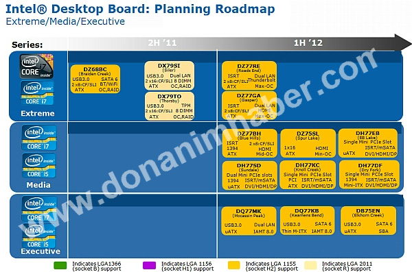
Intel DZ77RE First and Only to Feature Thunderbolt from Intel's 7-series Board Stable
This week, we got two important bits of news, firstly, that Intel's
third-generation Core processor family (codenamed "Ivy Bridge"), is
scheduled for launch on April 8, 2012; and secondly, that Intel will use
that occasion to launch its new 7-series chipset, and with it, bring
its 10 Gbps Thunderbolt interconnect to the PC platform. A road-map
slide tabling Intel's own Desktop Board division products based on
7-series chipset, shows that only one motherboard from Intel's stable
will feature Thunderbolt, the DZ77RE.
The DZ77RE is likely listed within the Extreme Series, which will be a top-of-the-line product. This is a bit of a contradiction to the idea behind Thunderbolt, and the way Intel's Desktop Board lineup is designed. It typically consists of Extreme Series, geared for gamers and overclockers; Media Series, for content-creation professionals; Classic Series, for office PCs with room for upgrades; and Essential Series, which well, covers the essentials. None of the supposed Media Series boards from Intel's 7-series chipset based Desktop Board lineup is listing Thunderbolt support, when it's the content-creation industry that stands to be the primary user of the interface. Thunderbolt facilitates ultra-high bandwidth for multiple lossless high-resolution video streams which will help in tomorrow's video-editing systems.
Sources: Expreview, DonanimHaber
The DZ77RE is likely listed within the Extreme Series, which will be a top-of-the-line product. This is a bit of a contradiction to the idea behind Thunderbolt, and the way Intel's Desktop Board lineup is designed. It typically consists of Extreme Series, geared for gamers and overclockers; Media Series, for content-creation professionals; Classic Series, for office PCs with room for upgrades; and Essential Series, which well, covers the essentials. None of the supposed Media Series boards from Intel's 7-series chipset based Desktop Board lineup is listing Thunderbolt support, when it's the content-creation industry that stands to be the primary user of the interface. Thunderbolt facilitates ultra-high bandwidth for multiple lossless high-resolution video streams which will help in tomorrow's video-editing systems.
Sources: Expreview, DonanimHaber
Wednesday, December 21, 2011
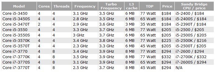
Intel 'Ivy Bridge' Core Desktop Processor Prices Compiled
In 2012, Intel will update its processor lineup up to performance 2
tiers with new models based on the spanking new 22 nm "Ivy Bridge"
silicon, which will increase performance over the current generation,
and bring some new features to the table. In late November, a list of
desktop Core i5/i7 models could be compiled, which were later confirmed on roadmap slides.
CPU World compiled retail channel pricing of several of those Core
i5/i7 "Ivy Bridge" chips. The prices look to be more or less consistent
with current "Sandy Bridge" Core processors, which those chips are
bound to replace. The Core i7-3770K, for example, which will replace the
Core i7-2600K, will be similarly priced to it.
Source: CPU-World
Source: CPU-World
Thursday, December 8, 2011
Intel to Retire its LGA1366 and LGA1156 Processors in 2012
These 45nm and 32nm CPUs are set to be available for further orders until June 29, 2012, and will continue to ship either until supplies are depleted (for the boxed versions) or until December 7th, 2012 (for the tray SKUs). As always, it's onwards and upwards.
Source
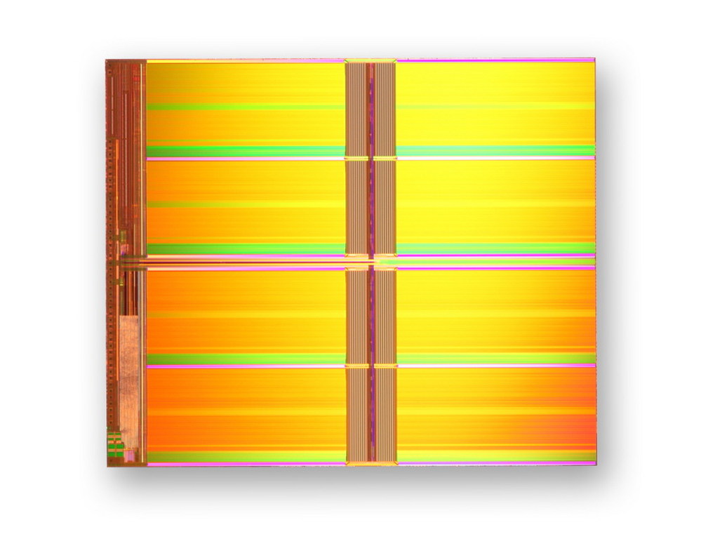
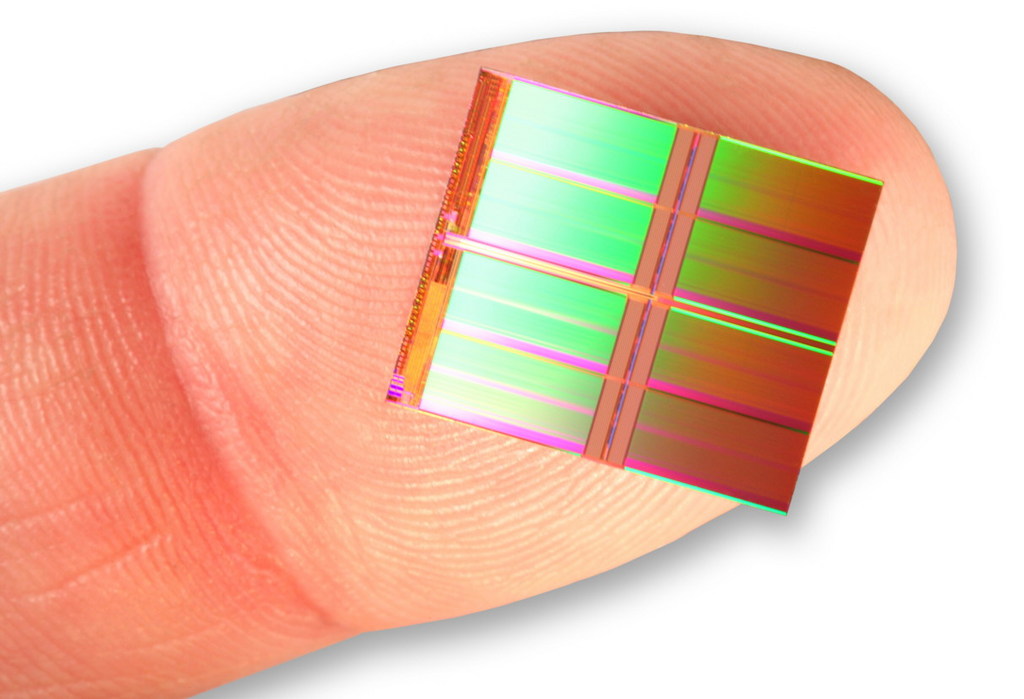
Intel and Micron develop first-ever 128 Gb NAND Flash memory chip
Flash buddies Intel
and Micron have today announced a significant breakthrough in terms of
NAND density, the first 128 Gb (16 GB) MLC NAND memory chip.
Manufactured on 20 nm process technology, this 128 Gb chip complies with
the ONFI 3.0 specification (enabling speeds of up to 333 megatransfers
per second) and can be used for new, high-capacity solid state drives,
as well as for next-generation tablets, smartphones and other portable
devices.
According to Intel and Micron, this milestone was made possible by the use of a new, innovative cell structure that 'breaks the scaling constraints of the standard NAND floating gate cell by integrating the first Hi-K/metal gate stack on NAND production.'
"It is gratifying to see the continued NAND leadership from the Intel-Micron joint development with yet more firsts as our manufacturing teams deliver these high-density, low-cost, compute-quality 20 nm NAND devices," said Rob Crooke, Intel vice president and general manager of Intel's Non-Volatile Memory Solutions Group. "Through the utilization of planar cell structure and Hi-K/Metal gate stack, IMFT continues to advance the technological capabilities of our NAND flash memory solutions to enable exciting new products, services and form factors."
IM Flash Technologies (the NAND joint venture of Intel and Micron) will have samples of the 128 Gb MLC chip in January and expects to start mass production in the first half of next year. In the mean time, the JV has ramped up mass production of its 64 Gb 20 nm NAND memory.
Source
According to Intel and Micron, this milestone was made possible by the use of a new, innovative cell structure that 'breaks the scaling constraints of the standard NAND floating gate cell by integrating the first Hi-K/metal gate stack on NAND production.'
"It is gratifying to see the continued NAND leadership from the Intel-Micron joint development with yet more firsts as our manufacturing teams deliver these high-density, low-cost, compute-quality 20 nm NAND devices," said Rob Crooke, Intel vice president and general manager of Intel's Non-Volatile Memory Solutions Group. "Through the utilization of planar cell structure and Hi-K/Metal gate stack, IMFT continues to advance the technological capabilities of our NAND flash memory solutions to enable exciting new products, services and form factors."
IM Flash Technologies (the NAND joint venture of Intel and Micron) will have samples of the 128 Gb MLC chip in January and expects to start mass production in the first half of next year. In the mean time, the JV has ramped up mass production of its 64 Gb 20 nm NAND memory.
Source
Saturday, December 3, 2011
Intel 2012 Core Processor Model Names Confirmed on Roadmap Slide
Earlier this week, a report tabled the model numbers of Intel's 2012 Core processor family based on the "Ivy Bridge" silicon. Its
processor model number scheme consisted of Core i5/i7 3000 series,
targeting various market price points. Many of these model numbers are
confirmed on the latest roadmap slide detailing the Core processor
family for 2012. We are also getting to see what the nomenclature of
next-generation Core i3 processors could look like.
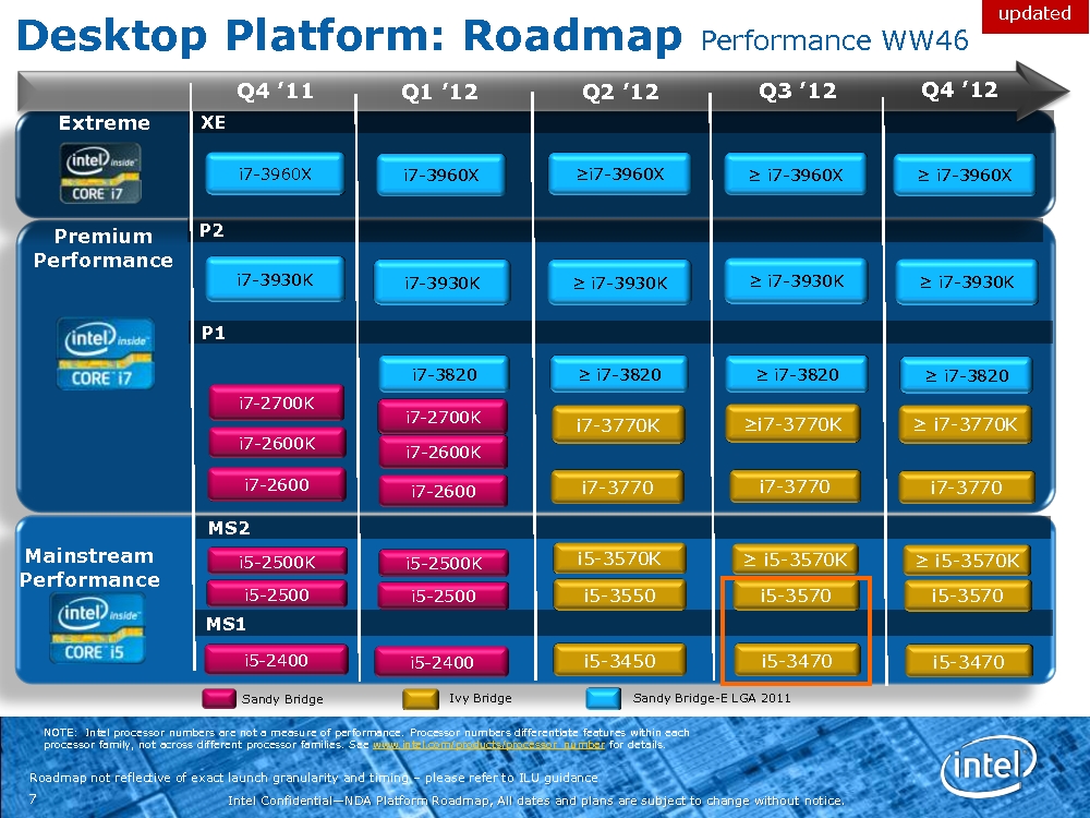
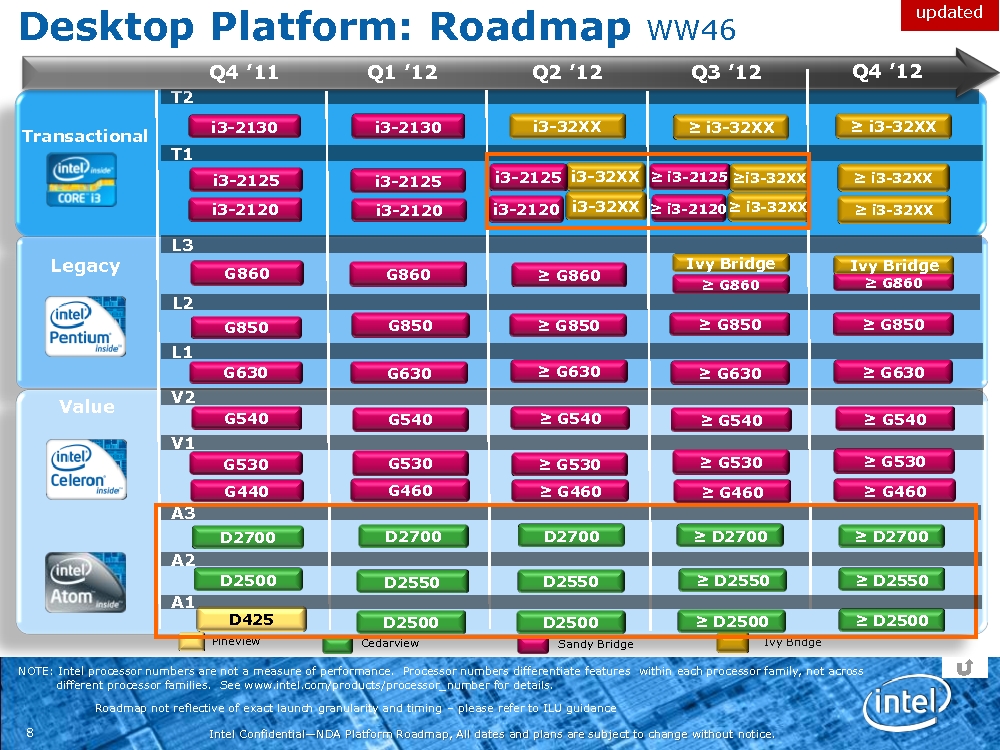
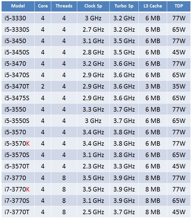
The slide shows that Ivy Bridge processors will start selling in Q2 2012, which is consistent with reports of an April 2012 launch. Intel will begin with Core i3-32xx (xx = TBD), i5-3450, i5-3550, i5-3570K, i7-3770, and i7-3770K. Around this time, there will be a market transition among cheaper Core i3 parts. In Q3 2012, i5-3470 and i5-3570 will displace i5-3450 and i5-3550; while a faster Core i7-37x0K processor will displace the i7-3770K. The market transition among some Core i3 parts will continue in Q3. Q4 2012 will largely resemble Q3, except that the lower-end Core i3 lineup will have fully transitioned to Ivy Bridge. There will be no changes in the LGA2011 Sandy Bridge-E HEDT lineup, except that an affordable quad-core part will be added in Q1 2012. For quick reference, we re-posted the table from the older report.
Source: VR-Zone
The slide shows that Ivy Bridge processors will start selling in Q2 2012, which is consistent with reports of an April 2012 launch. Intel will begin with Core i3-32xx (xx = TBD), i5-3450, i5-3550, i5-3570K, i7-3770, and i7-3770K. Around this time, there will be a market transition among cheaper Core i3 parts. In Q3 2012, i5-3470 and i5-3570 will displace i5-3450 and i5-3550; while a faster Core i7-37x0K processor will displace the i7-3770K. The market transition among some Core i3 parts will continue in Q3. Q4 2012 will largely resemble Q3, except that the lower-end Core i3 lineup will have fully transitioned to Ivy Bridge. There will be no changes in the LGA2011 Sandy Bridge-E HEDT lineup, except that an affordable quad-core part will be added in Q1 2012. For quick reference, we re-posted the table from the older report.
Source: VR-Zone
Saturday, November 26, 2011
New Intel Pentium Chip Headed for Low Cost Servers
Intel started shipping the new Pentium 350, a model designed specifically for
low-cost servers, micro-servers, and home servers; a segment Intel
originally planned to address with some of its Atom dual-core chips. The
Pentium 350 is an offshoot from entry-level desktop and notebook
platforms the Pentium brand is currently in charge of, it is designed
with durability and energy-efficiency required by servers in mind.
Available in the LGA1155 package, Pentium 350 is a dual-core processor based on the 32 nm Sandy Bridge dual-core silicon. It is clocked at 1.20 GHz, and features 3 MB of shared L3 cache apart from 256 KB L2 cache per core. Thanks to its low clock speed, the chip's TDP is rated at just 15W, making it ideal for home and small business servers. It will naturally benefit from the high IPC of Sandy Bridge architecture. The chip features Intel64 instruction set, its integrated memory controller supports up to 32 GB of dual-channel DDR3-1066/DDR3-1333 MHz memory.
Its on-chip graphics controller is disabled (so it relies on the one server boards come with, or any discrete graphics card). Moving on to its feature-set, HyperThreading Technology is available, enabling 4 logical CPUs for the operating system to deal with. The latest AVX instruction set is lacking, though SSE instruction sets up to SSE4.2 are available. VT-x finds room. Fast memory access, flex memory access, and NX-bit wrap it up. There is no word on the retail pricing.
Available in the LGA1155 package, Pentium 350 is a dual-core processor based on the 32 nm Sandy Bridge dual-core silicon. It is clocked at 1.20 GHz, and features 3 MB of shared L3 cache apart from 256 KB L2 cache per core. Thanks to its low clock speed, the chip's TDP is rated at just 15W, making it ideal for home and small business servers. It will naturally benefit from the high IPC of Sandy Bridge architecture. The chip features Intel64 instruction set, its integrated memory controller supports up to 32 GB of dual-channel DDR3-1066/DDR3-1333 MHz memory.
Its on-chip graphics controller is disabled (so it relies on the one server boards come with, or any discrete graphics card). Moving on to its feature-set, HyperThreading Technology is available, enabling 4 logical CPUs for the operating system to deal with. The latest AVX instruction set is lacking, though SSE instruction sets up to SSE4.2 are available. VT-x finds room. Fast memory access, flex memory access, and NX-bit wrap it up. There is no word on the retail pricing.
Subscribe to:
Posts (Atom)